DIODE CHARACTERISTICS AND PROPERTIES
A diode is one of the simplest semiconductor devices, which has the characteristic of passing current in one direction only. However, unlike a resistor, a diode does not behave linearly with respect to the applied voltage as the diode has an exponential Current - Voltage relationship and therefore we can not described its operation by simply using an equation such as Ohm's law.
1. PN JUNCTION:
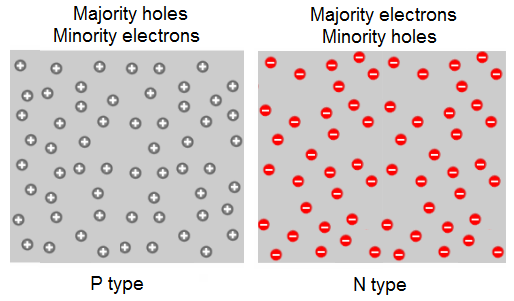
A P-N junction is formed by combining P-type and N-type doped semiconductors. When combined, a diffusion gradient is created. That is unevenness in the distribution of electrons and holes.
1.1.Holes and electrons diffusion:
It only makes sense that the holes are going to start to diffuse from the P region into the N region, and the electrons will diffuse from the N region into the P region.
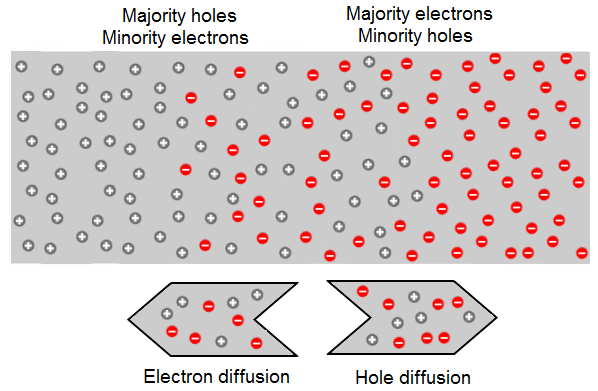
An equilibrium will be reached whereby electrons are diffusing out of the N-region, and drifting (pulled by the huge positive charge left behind) back in at exactly the same rate.
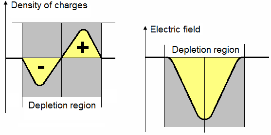
The electric field caused by the positive ions left behind prevents all of the electrons from diffusing out of the N-region.
1.2. Depletion region:
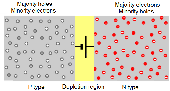
Consider an electron that diffuses out of the N-region. When it enters the P-region, it is met with a layer of negatively charged ions, and no holes (they all diffused into the N-region). So there's nothing for the electron to recombine with.
The same holds true for holes; a hole that diffuses into the N-region is met immediately with a region devoid of electrons, and full of positive ions. It can't recombine; it must wait until it reaches the N-type area, with its abundance of free electrons, to do so.
In semiconductor physics, the depletion region, also called depletion layer, depletion zone, junction region or the space charge region, is an insulating region within a conductive, where the mobile charge carriers have diffused away, or have been forced away by an electric.
2. DIODE CHARACTERISTICS:
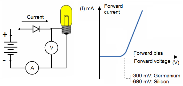
2.1. Forward-biased diode:
When the diode is forward-biased and conducting current, there is a small voltage dropped across it, leaving most of the battery voltage dropped across the resistor.
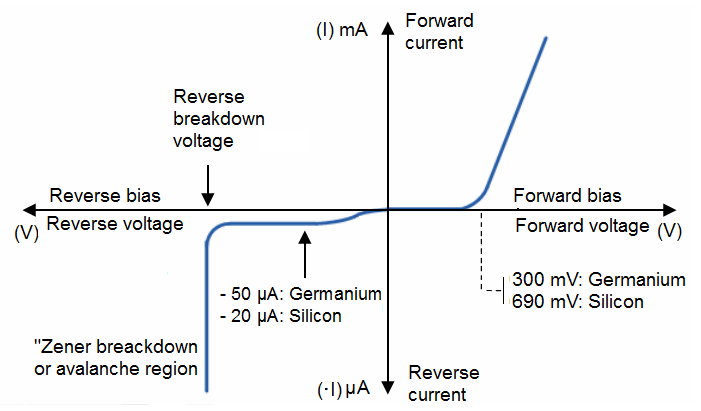
For silicon diodes, the typical forward voltage is 690 mV, nominal. For germanium diodes, the forward voltage is only 300 mV.
The chemical constituency of the P-N junction comprising the diode accounts for its nominal forward voltage figure, which is why silicon and germanium diodes have such different forward voltages.
Note - Influence of the temperature:
Also, since temperature is a factor in the diode characteristic. For the same value of the direct current, the anode-cathode tension decreases when the temperature increases.
For a silicon diode anode-cathode tension decreases about 2 mV/°C.
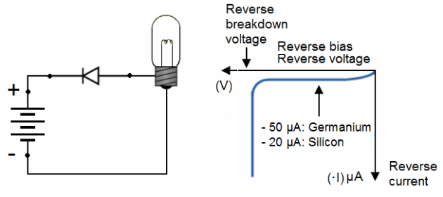
2.2. Reverse-biased diode:
When the battery's polarity is reversed and the diode becomes reverse-biased, it drops all of the battery's voltage and leaves none for the lamp. If we consider the diode to be a sort of self-actuating switch (closed in the forward-bias mode and open in the reverse-bias mode), this behaviour makes sense
2.3. Resume:
If a suitable positive voltage (forward bias) is applied between the two ends of the PN junction, it can supply free electrons and holes with the extra energy they require to cross the junction as the width of the depletion layer around the PN junction is decreased.
Then the depletion layer widens with an increase in the application of a reverse voltage and narrows with an increase in the application of a forward voltage. This is due to the differences in the electrical properties on the two sides of the PN junction resulting in physical changes taking place.
One of the results produces rectification as seen in the PN junction diodes static Current - Voltage.
3. DIODE MODELS:
This diode characteristic is quite fundamental to all of our work with semiconductors and we need to develop a "model" for its behaviour which allows a mathematical description. We are going to consider three levels of model complexity - starting off very simply as follows.
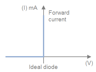
3.1. Ideal diode:
An ideal diode is like a light switch in your home.
When the switch is closed, the circuit is completed; and the light turns on.
When the switch is open, there is no current and the light is off.
However, the diode has an additional property; it is unidirectional, i.e. current flows in only one direction (anode to cathode internally).When a forward voltage is applied, the diode conducts; and when a reverse voltage is applied, there is no conduction.
An ideal diode characteristic would be:
![]()
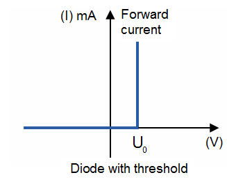
3.2. Diode with threshold:
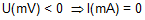
What this is saying is that if V is less than zero the PN diode is not conducting at all and the moment the applied voltage increases above zero the diode becomes a perfect conductor.
Translating that into Mathematics: If the voltage applied to the diode V is less than zero then current flow = zero; if the voltage applied to the diode is greater than zero then the current which flows is infinite.
Infinity is a bit unreal but what that is saying is that the model is a simple switch - it is either ON or it is OFF.
Forward voltage:
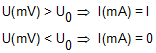
Reverse voltage:
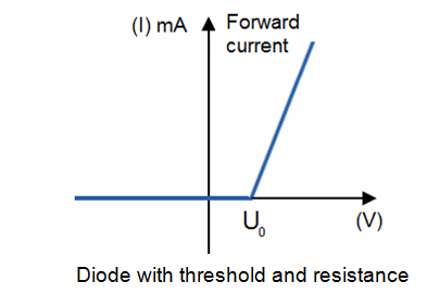
3.3. Diode with threshold and resistance characteristic:
The next more complicated model is shown in the following figure:
In this case the model appears like a 0.7 volt battery in series with a simple series resistor whose value is the (inverted value of!) the slope of this straight line.
Forward voltage:
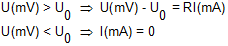
Reverse voltage: