OPERATION AND FUNCTION OF DIODES IN THE FOLLOWING CIRCUITS: CLIPPERS, CLAMPERS, FULL AND HALF WAVE RECTIFIERS, BRIDGE RECTIFIERS, VOLTAGE DOUBLERS AND TRIPLERS
1. CLIPPERS OR LIMITERS:
1.1. Biased simple-limiter:
Limiter is a wave shaping circuit used to limit ac voltage to predetermined level. Limiters can transform a sine wave into rectangular wave, can limit either the – Ve or +Ve alternation or both alternations of an ac voltage. The diode limiters are also known as clippers


Limiters may be classified as Series limiter and Parallel limiter depending on whether the output is taken from the load resistor in series with the diode or in parallel with it.
Diode will become forward biased as soon as VA becomes larger than VBIAS + 0.7.
When diode is forward biased, VA cannot become larger than VBIAS + 0.7 V. Thus, the voltage across the load, RL, will also be equal to VBIAS + 0.7.
When diode is reverse biased, it appears as an open, so the output voltage is the voltage of RL alone.
Desired voltage levels can be attained with a voltage divider. We replace the voltage source with a resistive voltage divider.
![]()
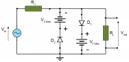
1.2. Biased double-limiter:
As shown in the above circuit diagram two biased diode limiters are connected in parallel such that the circuit acts as a partial limiter of both the alternations.
During the +V half cycle of the input voltage D1 remains in the reverse biased state. D2 also remains in the reverse biased state until the input voltage reaches the bias voltage V1bias + 0.7 V.
Thus the output voltage follows the input until D2 is forward biased.
Thereafter the output remains constant at V1bias + 0.7 V.
During the -V half cycle of the input voltage D2 remains in the reverse biased state. D1 also remains in the reverse biased state until the input voltage becomes more -Ve than the bias voltage V2bias + 0.7 V.
Thus the output voltage follows the input until D1 is forward biased.
Thereafter the output remains constant at V2bias + 0.7 V.
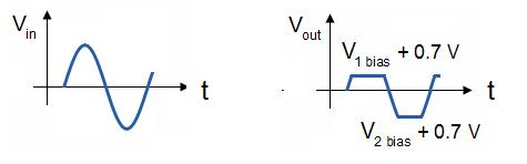
Thus the diode limiter modifies the input waveform by limiting part of that waveform thereby changing the shape of the input waveform whose extremities has been squared off.
The output waveform may be observed in the waveform viewer.
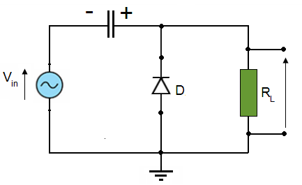
2. DIODE CLAMPERS:
Certain applications in electronics require that the upper or lower extremity of a wave be fixed at a specific value. In such applications, a clamping (or clamper) circuit is used.
A clamping circuit clamps or restrains either the upper or lower extremity of a waveform to a fixed dc potential.
This circuit is also known as a direct-current restorer or a base-line stabilizer.
Such circuits are used in test equipment, radar systems, electronic countermeasure systems, and sonar systems. Depending upon the equipment, you could find negative or positive clampers with or without bias.
Consider the circuit shown with a time constant RC much greater than the time period T of the input waveform.
For all practical purposes, let us assume that this condition is met as long as RC > 10T.
2.1. This is how this circuit works:
a) During the negative half-cycle of the input waveform, the diode is reverse-biased and the capacitor cannot charge through due to its large time constant.
Thus, the capacitor voltage stays basically at zero. Hence, the output voltage is the same as the input voltage.
b) During the positive half-cycle, the diode is forward biased. For an ideal diode, the capacitor charges to its maximum value of with the polarity as shown.
The output voltage is zero as the ideal diode is now conducting.
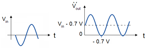
Capacitor charges to near peak of input V+ = VIN - 0.7 V..
c) During the next negative half-cycle, the diode is reverse-biased again. The output voltage is algebraic sum of the voltage across the capacitor and the input voltage. During this cycle, the capacitor cannot discharge owing to its large time constant again. From now onward, the capacitor voltage stays at with the polarity as shown in the figure. Thus, the capacitor behaves like a constant voltage source whose value is equal to the maximum value of the input voltage source for an ideal diode in the circuit.
The input and the output voltage waveforms are given in figure.
Note: The output voltage has shifted up, its minimum value is zero, and the maximum value is .
Once again, note that the shift is in the direction of the arrow of the diode. Since there is no voltage source in series with the diode, the minimum output voltage under deal condition is zero.
2.2. Other examples of clamping currents:
In function of the form of the input current, we can obtain various output clamping currents:

3. POWER DIODES AND RECTIFIERS:
3.1. Power diodes:
We saw that a semiconductor signal diode will only conduct current in one direction from its anode to its cathode (forward direction), but not in the reverse direction acting a bit like an electrical one way valve.
A widely used application of this feature is in the conversion of an alternating voltage (AC) into a continuous voltage (DC).
Small signal diodes can be used as rectifiers in low-power, low current (less than 1-amp) rectifiers or applications, but were larger forward bias currents or higher reverse bias blocking voltages are involved the PN junction of a small signal diode would eventually overheat and melt so larger more robust power diodes are used instead.
Power diodes are designed to have a forward "ON" resistance of fractions of an Ohm while their reverse blocking resistance is in the mega-Ohms range.
Some of the larger value power diodes are designed to be "stud mounted" onto heat sinks reducing their thermal resistance to between 0.1 to 1oC/Watt.
If an alternating voltage is applied across a power diode, during the positive half cycle the diode will conduct passing current and during the negative half cycle the diode will not conduct blocking the flow of current.
Then conduction through the power diode only occurs during the positive half cycle and is therefore unidirectional i.e. DC as shown.
3.2. Half-wave rectifier:
a) First alternance:
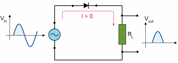
During the half cycle when the diode is forward-biased:
![]()
Where VT is the threshold voltage of the diode.
b) Second alternance:

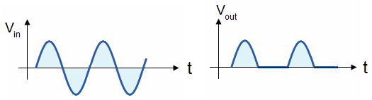
During the half cycle when the diode is reverse-biased Vout = O V.
c) Alternative current:
3.3. Full-wave rectifier:
Half-wave rectifiers have some applications.
However, full-wave rectifiers are the most commonly used ones for DC power supplies.
A full-wave rectifier is exactly the same as the half-wave, but allows unidirectional current through the load during the entire sinusoidal cycle (as opposed to only half the cycle in the half-wave).
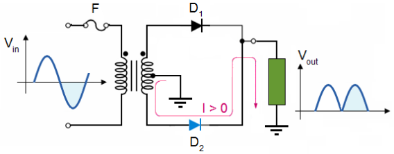
During negatives half-cycles, D1 is reverse-biased and D2 is forward-biased.
3.4. Bridge rectifiers:
A bridge rectifier can be made using four individual diodes, but it is also available in special packages containing the four diodes required. It is called a full-wave rectifier because it uses all the AC wave (both positive and negative sections).
1.4 V is used up in the bridge rectifier because each diode uses 0.7 V when conducting and there are always two diodes conducting, as shown in the diagram below.
Bridge rectifiers are rated by the maximum current they can pass and the maximum reverse voltage they can withstand (this must be at least three times the supply RMS voltage so the rectifier can withstand the peak voltages).

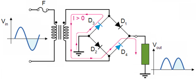
During positives half-cycles of the input, D1 and D2 are forward-biased and conduct the current. D3 and D4 are reverse-biased and don't conduct.
During negatives half-cycles of the input, D1 and D2 are reverse-biased and doesn't conduct the current. D3 and D4 are forward-biased and conduct.
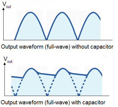
3.5. Adding a smoothing capacitor:
Smoothing is performed by a large value electrolytic capacitor connected across the DC supply to act as a reservoir, supplying current to the output when the varying DC voltage from the rectifier is falling. The diagram shows the unsmoothed varying DC (dotted line) and the smoothed DC (solid line).
The smoothing capacitor converts the wave rippled output of the rectifier into a smooth DC output voltage.
Generally for DC power supply circuits the smoothing capacitor is an Aluminium Electrolytic type that has a capacitance value of 100uF or more with repeated DC voltage pulses from the rectifier charging up the capacitor to peak voltage.
However, their are two important parameters to consider when choosing a suitable smoothing capacitor and these are its Working Voltage, which must be higher than the no-load output value of the rectifier and its Capacitance Value, which determines the amount of ripple that will appear superimposed on top of the DC voltage.
Too low a value and the capacitor has little effect but if the smoothing capacitor is large enough (parallel capacitors can be used) and the load current is not too large, the output voltage will be almost as smooth as pure DC.
As a general rule of thumb, we are looking to have a ripple voltage of less than 100mV peak to peak.
4. VOLTAGE MULTIPLIERS:
Voltage multipliers use clamping action to increase peak rectified voltages without increasing input transformer's rating.
Multiplication factors of 2, 3, and 4 are common.
They are used in high-voltage, low-current applications.
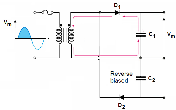
4.1. Voltage doubler:
There are two types of voltage doublers:
Half-wave doubler,
Full-wave doubler.
a) Half-wave doubler:
During the positive half-cycle of the secondary voltage, diode D1 is forward-biased and D2 is reverse-biased. Capacitor C1 is charged to the peak of the secondary voltage VM less diode drop.

During the negative half-cycle, diode D2 is forward-biased and D1 is reverse-biased. C1 cannot discharge.
Thus, C1's voltage adds to the secondary voltage to charge C2 to approximately 2VM .
Under no-load conditions, C2 remains charged. If load is added, C2 will discharge through load on the next positive half-cycle only to be recharged in the following negative half-cycle.
Resulting wave is a half-wave, capacitor-filtered voltage. PIV across each diode is 2VM.

b) Full-wave doubler:
During the positive half-cycle, D¬1 is forward biased and C1 charges to approximately VM.
During the negative half-cycle, D2 is forward biased and C2 charges to approximately VM.
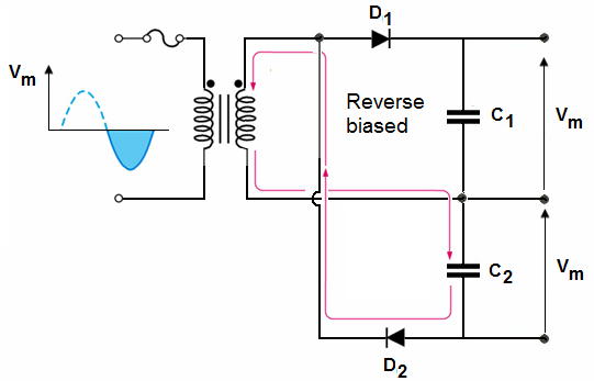
Output voltage is tasked across the two capacitors in series.
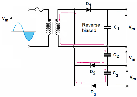
4.2. Voltage tripler:
Exactly like the half-wave doubler, but another diode-capacitor pair is added.
During the negative half-cycle: