P AND N TYPE MATERIALS: EFFECTS OF IMPURITIES ON CONDUCTION, MAJORITY AND MINORITY CHARACTERS
1. EFFECTS OF IMPURITIES ON CONDUCTION:
A common method for generating even more charge carriers in a semiconductor is by doping. That is, replacing a few atoms of the base material with atoms of a different element.
These impurities will contribute an excess electron or hole which is loosely bound and hence can be excited into the conduction band by thermal energy.
For example, doped junction silicon crystal with adjoining P-type substances (aluminum, gallium) and N-type substances (phosphorus, arsenide) is used to form a diode.


The key thing about these semiconductor materials is that we can very carefully and precisely introduce impurities and this leads to the development of extraordinarily useful devices for electronic applications.
This process is known as "DOPING".
2. MAJORITY AND MINORITY CHARACTERS:
The doping process introduces extremely precise concentrations of elements:
from Column 3 of the periodic table: P–Extrinsic elements (P or Positive),
from Column 5 of the periodic table: N–Extrinsic elements (N or Negative).
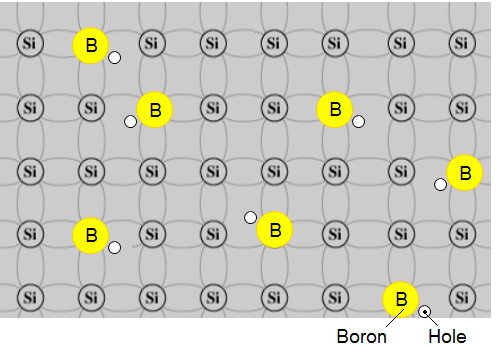
2.1. P-Extrinsic semiconductor:
In P-type doping, boron (B) or gallium (Ga) is the dopant. Boron and gallium each have only three outer electrons.
When mixed into the silicon lattice, they form “holes” in the lattice where a silicon electron has nothing to bond to. The absence of an electron creates the effect of a positive charge, hence the name P-type.
Holes can conduct current. A hole happily accepts an electron from a neighbour, moving the hole over a space.
Example - boron p-type:
Typical of these is boron from column 3 and arsenic from Column 5.
Use the 2-D representation of pure Silicon with each atom sharing electrons with 4 adjacent atoms as shown next figure:
We show an atom of boron which has just three electrons in its outer most shell before it enters the silicon arrangement.
The next sketch depicts the doped material:
It is easy to see that the newly embedded boron atom introduces an available "hole" into the silicon structure but the whole material is electrically stable, particularly at absolute zero of temperature.
2.2. N-Extrinsic semiconductor:
In N-type doping, phosphorus (P) or arsenic (As) is added to the silicon in small quantities.
Phosphorus and arsenide each have five outer electrons, so they're out of place when they get into the silicon lattice.
The fifth electron has nothing to bond to, so it's free to move around. It takes only a very small quantity of the impurity to create enough free electrons to allow an electric current to flow through the silicon.
N-type silicon is a good semiconductor.
Electrons have a negative charge, hence the name N-type.
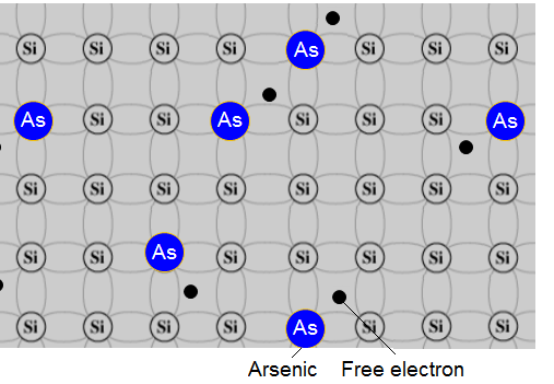
Example - arsenic n-type:
The sequence of doping with arsenic shows the atom of arsenic which has 5 electrons in its outermost shell before it enters the pure silicon. Four of them are used to covalent links and the fifth is a free electron.