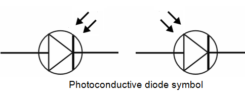
DETAILED OPERATION AND CHARACTERISTICS OF PHOTOCONDUCTIVE DIODES
A photo-conductive diode is a diode optimized to produce an electron current flow in response to irradiation by ultraviolet, visible, or infrared light. Silicon is most often used to fabricate photodiodes; though, germanium and gallium arsenide can be used.
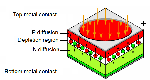
The junction through which light enters the semiconductor must be thin enough to pass most of the light on to the active region (depletion region) where light is converted to electron hole pairs.

In Figure a shallow P-type diffusion into an N-type wafer produces a PN junction near the surface of the wafer. The P-type layer needs to be thin to pass as much light as possible.
A heavy N+ diffusion on the back of the wafer makes contact with materialization. The top metalization may be a fine grid of metallic fingers on the top of the wafer for large cells. In small photodiodes, the top contact might be a sole bond wire contacting the bare P-type silicon top.
4.1. Mechanism of conduction:
Light entering the top of the photodiode stack fall off exponentially in with depth of the silicon. A thin top P-type layer allows most photons to pass into the depletion region where electron-hole pairs are formed.
The electric field across the depletion region due to the built in diode potential causes electrons to be swept into the N-layer, holes into the P-layer. Actually electron-hole pairs may be formed in any of the semiconductor regions. However, those formed in the depletion region are most likely to be separated into the respective N and P-regions.
Many of the electron-hole pairs formed in the P and N-regions recombine. Only a few do so in the depletion region. Thus, a few electron-hole pairs in the N and P-regions, and most in the depletion region contribute to photocurrent, that current resulting from light falling on the photodiode.
4.2. Applications-Solar cells:
A photodiode optimized for efficiently delivering power to a load is the solar cell. It operates in photovoltaic mode (PV) because it is forward biased by the voltage developed across the load resistance.
Monocrystalline solar cells are manufactured in a process similar to semiconductor processing. This involves growing a single crystal boule from molten high purity silicon (P-type), though, not as high purity as for semiconductors. The boule is diamond sawed or wire sawed into wafers. The ends of the boule must be discarded or recycled, and silicon is lost in the saw kerf. Since modern cells are nearly square, silicon is lost in squaring the boule. Cells may be etched to texture (roughen) the surface to help trap light within the cell. Considerable silicon is lost in producing the 10 or 15 cm square wafers. These days (2007) it is common for solar cell manufacturer to purchase the wafers at this stage from a supplier to the semiconductor industry.
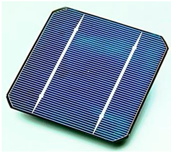
P-type Wafers are loaded back-to-back into fused silica boats exposing only the outer surface to the N-type doping in the diffusion furnace. The diffusion process forms a thin n-type layer on the top of the cell. The diffusion also shorts the edges of the cell front to back. The periphery must be removed by plasma etching to unshort the cell. Silver and or aluminum paste is screened on the back of the cell, and a silver grid on the front. These are sintered in a furnace for good electrical contact.
The cells are wired in series with metal ribbons. For charging 12 V batteries, 36 cells at approximately 0.5 V are vacuum laminated between glass, and a polymer metal back. The glass may have a textured surface to help trap light.