PN JUNCTION IN A SEMICONDUCTOR, DEVELOPMENT OF A POTENTIAL ACROSS A PN JUNCTION IN UNBIASING, FORWARD BIASING AND REVERSE BIASING CONDITIONS
1. REMINDER JUNCTIONS IN THE FIRST PART OF THIS LESSON.
2. UNBIASED PN JUNCTION:
The depletion region is thereby depleted of mobile charge carriers as a thermal equilibrium is reached, and a barrier is created between the n-type and p-type regions.
As argued above, there is also an electric field produced in this region due to the produced net positive and negative charges. This field typically has a magnitude between 1000 and 10000 V/cm.

This separation of charges develops a potential across the depletion region, preventing further diffusion of carriers across the junction.
This potential, known as the potential barrier, is about 0.7 V in a typical silicon P-N junction.
3. BIASED PN JUNCTION:
Then we apply a DC voltage to a PN junction - indeed to any semiconductor device - it is known as "biasing" that component. The behavior of a diode depends on its polarity in the circuit.
The potential may be applied in either:
a reverse potential difference,
a forward potential difference.
3.1. Reverse-biased PN junction:
We connect an external battery connected to our PN diode so that the positive goes to the P side and obviously the battery negative to the N side. The holes being positively charged will move towards the negative terminal while the electrons will move towards the positive terminal.
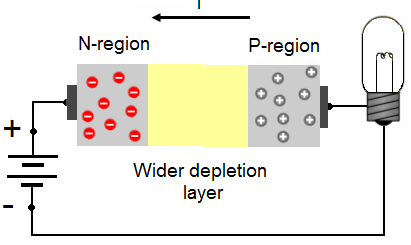
This will increase the thickness of the depletion layer so only a very small current can flow (probably due to the intrinsic carrier concentration). Under these set of circumstances, the diode is said to be in reverse bias
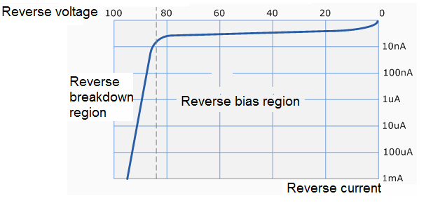
Theoretically, we could apply an infinite negative voltage to the P-side, and the device would not conduct. In fact, after a certain degree of reverse bias, the junction will go into what's known as “breakdown”. This typically occurs at voltages in the neighbourhood of 250V (reversed biased).
In reverse-biased montage:
the depletion region increases,
the density of charge in depletion region increases,
the electric field increases,
the voltage of virtual battery increases.
The only charge carriers able to support a net current across the PN junction are the minority carriers and hence the reverse current is very small, Ir = 0 A.
Reverse characteristic:
Note:
Sometimes this avalanche effect has practical applications in voltage stabilising circuits where a series limiting resistor is used with the diode to limit this reverse breakdown current to a preset maximum value thereby producing a fixed voltage output across the diode.
These types of diodes are commonly known as Zener Diodes and are discussed in a later tutorial.
3.2. Forward-biased PN junction:
A forward-biased diode (positive potential on P-type material) has a decreased depletion region; the majority carriers can diffuse across the junction.

The holes will flow away from the positive terminal and the electrons will flow away from the negative terminal. Remember that in current flow, all the like charges have to flow in the same direction. A hole moving away from the positive terminal is analogous to an electron moving towards the positive terminal. Since electrons are flowing from the negative terminal and towards the positive terminal, this implies that a sizable current is flowing through the diode.
By applying direct voltage to the P-type side, we've forward biased our junction. The hill is that much smaller, but we're not quite there yet. The magic happens when we apply a voltage equal to, or greater than the built-in voltage. Watch what happens if we connect a battery.
The flood gates are open, and electrons start to pour across the barrier in huge quantities. Not only are they diffusing across the depletion region at a high rate, but now that the electric field is reversed, they're also being accelerated across.
Because there's such a high concentration of electrons in the N-type region, the diffusion currents are extremely strong, and electrons flow at an enormous rate (i.e., large current).
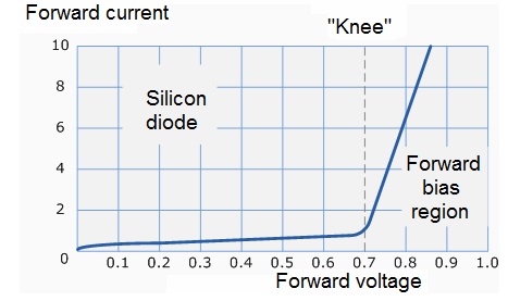
Essentially, the depletion region keeps narrowing until the “threshold” voltage (0.7 V) is met, as which time the depletion region disappears.
Holes do the same, in the opposite direction, of course. The current through the sample will increase exponentially as the voltage (forward biasing) increases; so fast, in fact, that if there is no external circuit in place to control the flow (a resistance), the current would increase so much that the junction would burn and destroy itself.
The voltage may become high enough to eliminate the depletion region entirely. Essentially, we now have a device that, if subjected to any voltage under 0.7 V (Threshold voltage), will not conduct, but once exposed to greater than 0.7 V, will conduct very well.
In forward-biased montage:
the depletion region decreases to get 0 at threshold voltage,
the density of charge in depletion region decreases to get 0 at threshold voltage,
the electric field decreases to get 0 at threshold voltage, the voltage of virtual battery decreases to get 0 at threshold voltage.
the voltage may become high enough when the depletion region is entirely eliminated.
Forward characteristic: