MATERIAL, ELECTRON CONFIGURATION, ELECTRICAL PROPERTIES
1. MATERIAL:
All matter is made of atoms.
Atoms consist of a small positive nucleus surrounded by a cloud of negative electrons.
Electrically neutral (not charged) matter has equal or balanced amounts of positive nuclei and surrounding negative electrons.
Electrons are arranged around the nucleus in layers or shells. The outer shell is the important one for chemistry, electronics and semiconductor manufacturing.
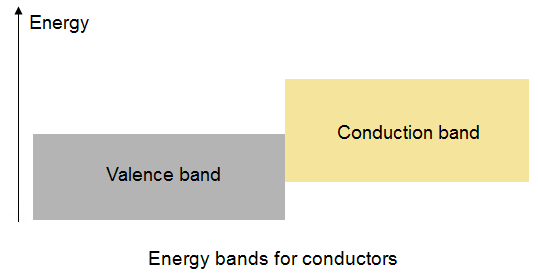
In crystals atoms interact and bind by sharing valence electrons. The wave function is no longer associated with a single atom but extends over the entire crystal. One effect of the interaction between the atoms is that the otherwise degenerate energy levels split into closely spaced levels. Since the number of atoms is large, it is common to refer to this set of levels as a continuous energy band.
In a solid material there exists:
a valence band which is an energy region where the states are filled by valence electrons.
a conduction band is defined to be the lowest unfilled energy band. So our three materials can be characterized by their band structure.
Conduction (free) electron: if an electron that has been pulled away from the valence shell is a free electron. Free electrons are very important in electricity, as free electrons generate electronic flows. The flow of free electrons yields an electric current. Once the valence electrons are pulled away, they are called free electrons. It's the movement of the free electrons that provides an electric current.
Valence electrons: In general, electrons closed to the nucleus and others are farther away:
Electrons in the inner shells near the nucleus are bound tightly to the atom.
Electrons in the outermost (valence) shell are loosely bound and may be pulled away from the nucleus by an outside force.
1.1. Conductors:
If there are few electrons in the valence shell, one electron can easily break loose.
Generally a conductor is a material that has 1, 2 or 3 valence electrons. For example, Aluminum is a conductor, as it has 3 electrons in its valence shell.
An atom with one valence electron is the best conductor.
All metals are conductors. But some metals are better conductors than others. The best conductors are silver, copper, and gold. Each of these metals has one electron in its valence shell.
1.2. Insulators:
Generally an insulator is a material that has 6, 7 or 8 valence electrons. An atom with eight valence electrons is stable, resists electron gain or loss, and is the best insulator. Such an atom is sometimes called “inert atom”.

1.3. Semiconductors:
If some thermally excited electrons can move from the valence band to the conduction band and conduct current.
Silicon and germanium have thermally excited electrons at room temperature and hence their common use in diodes and transistors.
Atoms with four valence electrons are semiconductors.
An interesting property of semiconductors is that when they are subjected to an increase in temperature, they tend to become conductors. When their temperature is very low, they tend to become insulators.

2. ELECTRON CONFIGURATION AND ELECTRICAL PROPERTIES:
Electrons move in orbits (called shells) around the nucleus like the planets around the sun. You can notice that each shell can only hold a certain number of electrons:
the first shell (close to the nucleus) cannot hold more than 2 electrons,
the second shell not more than 8,
the third shell not more than 18,
the fourth shell not more 32,
and so on.
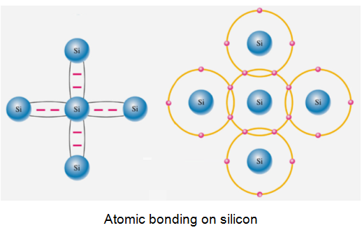
2.1. The atom of silicon:
The silicon atom has 14 electrons, 14 protons and 14 neutrons:
Its electrons are distributed as follows: 2 electrons are in the first shell.
The second shell of the silicon atom is full and contains eight electrons.
The third shell contains 14 – 2 – 8 = 4 electrons. The third shell is here again the valence shell.

2.2. Intrinsic (pure) semiconductor and thermal energy:
Intrinsic semiconductor is made of a pure crystal.
The physical principles of intrinsic semiconductor devices can be understood by considering quantum energy levels in the material. I will just give a sketchy view here and define some terminology.
A semiconductor has the valence band close to the conduction band - separated by about a 1 eV gap. Conductors on the other hand have the conduction and valence bands overlapping.
Germanium and Silicon (Column 4 elements) have four electrons in their outer shell. They are relatively poor conductors - which is why they are called SEMICONDUCTORS but it turns out that they have extraordinary properties which we can manipulate to our advantage.
They exist in a crystalline form in what is known as a "Diamond Cubic Lattice" structure.
The most common crystal structure among frequently used semiconductors is the diamond lattice. Each atom in the diamond lattice has a covalent bond with four adjacent atoms, which together form a tetrahedron. The diamond lattice therefore is a face-centred-cubic lattice with a basis containing two identical atoms.

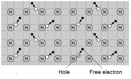
The interesting property of a semiconductor is that thermally excited electrons can move from the valence band to the conduction band and conduct current.
Silicon and germanium have thermally excited electrons at room temperature and hence their common use in diodes and transistors.
At absolute 0° K :
At absolute zero (- 273 degrees Centigrade) all of the bonds in the material are "frozen" in place and NO current will flow; it is then a perfect insulator.
At room temperature (300 °K):
As the temperature is increased the lattice structure begins to vibrate as it absorbs the heat energy and electrons can break free from the bonds - ever more so as the temperature is increased.
2.3. Free electrons, holes conduction:
When an electron has been excited into the conduction band, the hole left behind in the valence band is also free to move through the crystal. A quantum mechanical treatment of this effect puts the hole on an approximately equal footing with the electron. Temperature causes the thermal generation of electron-hole pairs.
When the electron has escaped it leaves behind a positive charge which has been called a "hole" since the broken bond wants to attract back the missing electron.
These holes themselves wander through the crystal lattice in the same way as electrons do and consequently they contribute directly to the current flow. In the pure or intrinsic material the number of free electrons equals the number of free holes.
One of the components of the pair will add a little to the majority charge carriers. The other component of the electron-hole pair will become the minority charge carrier. Minority charge carriers limit ideal performance and increase with increasing temperature.

It is interesting to look at what happens if we connect a piece of pure (intrinsic) semiconductor to a battery through wires.
In the copper wires the current flow is due only to electrons. Inside the semiconductor the number of electrons and holes must be exactly equal (because we are considering an absolutely pure = "intrinsic" semiconductor) so in there the current must be carried half by electrons and half by holes.
Electrons move from semiconductor to + POLE then generate a direct flow current from anode to copper.
Holes move from semiconductor to – POLE. The recombination with electron-copper generates in cupper an additional flow of electrons equal at direct flow.
2.2 Concentration P of electrons-holes in an intrinsic semiconductor:
In pure Silicon there are about 5. 1028 atoms per cubic meter.
For pure Silicon at room temperature (conventionally taken as 27 degrees Centigrade = 300 degrees Kelvin) there are about Ne = 1.5.1016 electrons available and obviously the same number of holes: Nh = 1.5.1016.
It has been found that the product P = of the number of electrons times the number of holes forms an important constant at a particular temperature: the concentration of electrons-holes.
For pure Silicon at "room" temperature: P =![]() .
.