DETAILED OPERATION AND CHARACTERISTICS OF THE SILICON CONTROLLED RECTIFIER
1. THYRISTOR:
The thyristor family of semiconductors consists of several very useful devices. The most widely used of this family are silicon controlled rectifiers (SCRs). There are many applications where these devices perform key functions and are real assets in meeting environmental, speed, and reliability specifications which their electro-mechanical counterparts cannot fulfil.
The purpose of this lesson is to better acquaint users of SCRs to the basic fundamentals of the thyristor.
1.1. Silicon controlled rectifier (SCR):
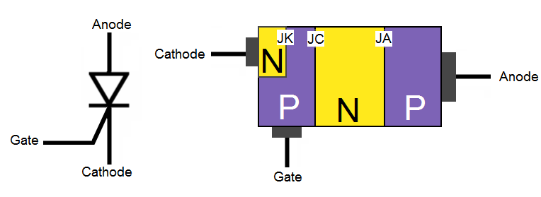
The SCR is a four layer three terminal device with junctions JK JC JA as shown. The construction of SCR shows that the gate terminal is kept nearer the cathode. The approximate thickness of each layer and doping densities are as indicated in the figure. In terms of their lateral dimensions
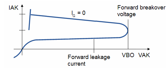
1.2. Thyristor characteristics:
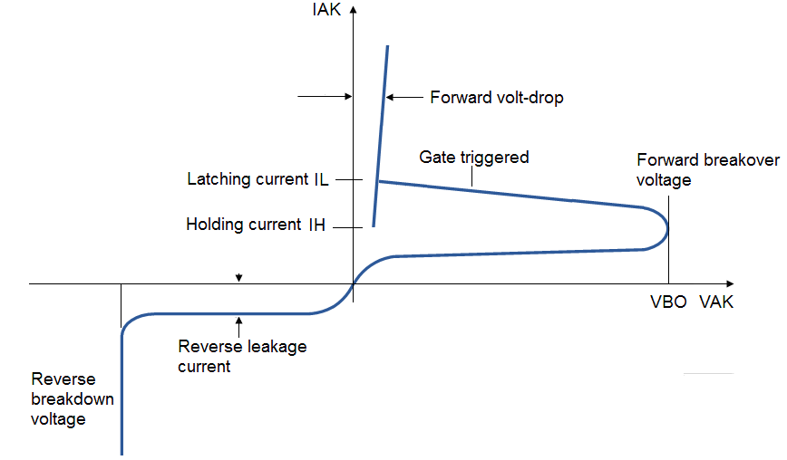
The important points on this characteristic are:
Latching current IL: This is the minimum anode current required to maintain the thyristor in the on-state immediately after a thyristor has been turned on and the gate signal has been removed.
Holding current IH: This is the minimum anode current required to maintain the thyristor in the on-state.
Forward breakover voltage VBO: If the forward voltage VAK is increased beyond VBO, the thyristor can be turned on. But such a turn-on could be destructive.
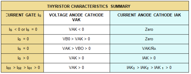
a) Reverse direction for zero gate current IG = 0 or IG < 0:
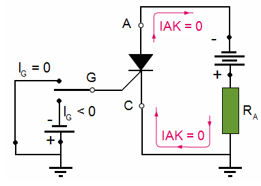
In the reverse direction the thyristor appears similar to a reverse biased diode which conducts very little current (leakage current: about few mA) until avalanche breakdown occurs.
b) Forward direction for zero gate current ( IG = 0):
In the forward direction the thyristor has two stable states or modes of operation that are connected together by an unstable mode that appears as a negative resistance on the characteristics.
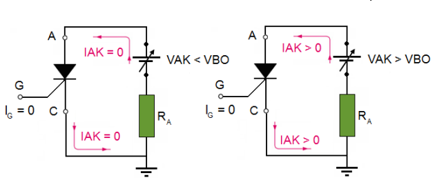
The low current high voltage region is the forward blocking state or the off state and the low voltage high current mode is the on state.
For the forward blocking state the quantity of interest is the forward blocking voltage VBO which is defined for zero gate current.
When the voltage anode–cathode VAK < VBO, the current IAK is zero. The thyristor is similar an open switch.
When the voltage anode–cathode VAK > VBO, the current IAK is positive. The thyristor is similar a shunt.
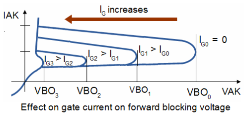
c) Forward direction for gate current positive (IG > 0):
If a positive gate current is applied to a thyristor then the breakover to the on state will occur at smaller values of anode to cathode voltage as shown.
Although not indicated the gate current does not have to be a DC current but instead can be a pulse of current having some minimum time duration. This ability to switch the thyristor by means of a current pulse is the reason for wide spread applications of the device.
1.3. Thyristor applications:
The curves show that the SCR's forward breakover voltage decreases as the gate current increases. In fact, the gate current could be increased to a value (IG3) where the breakover voltage would be so low that the device would have characteristics that closely resemble those of an ordinary PN junction diode.
This ability of the gate to control the point where breakover occurs is used to advantage in many types of electronic circuits.
The curves reveal much about the SCR's most important electrical characteristics.
Basically these curves show that for any given gate current, a specific forward breakover voltage must be reached before the SCR can turn on.
However, the curves also show that for any given forward voltage across the SCR, a specific value of gate current must be reached before the device can turn on.
Therefore, an SCR can be turned on only when it is subjected to the proper combination of gate current and forward voltage values.
a) Thyristor as a switch:
The SCR is primarily used to control the application of DC or AC power to various types of loads.
It can be used as a switch to open or close a circuit or it can be used to vary the amount of power applied to a load.
A very low current gate signal can control a very large load current. The SCR is basically used as a switch to apply DC power to the load resistor. The switch could be momentarily closed to short out the SCR and reduce its anode-to-cathode voltage to zero.
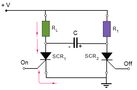
A more practical SCR circuit is shown in Figure below.
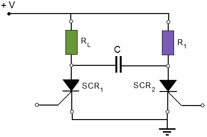
With this circuit, mechanical switches have been completely eliminated.
In this circuit SCR1 is used to control the DC power applied to load resistor RL and SCR2 along with a capacitor (C) and a resistor R1 are used to turn off the circuit.
When a momentary gate current flows through SCR1, this SCR turns on and allows a DC voltage to be applied to RL.
This effectively grounds the left hand side of capacitor C and allows it to charge through resistor R1:
Right plate of capacitor > 0,
Left plate of capacitor < 0,
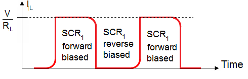
When a momentary gate current pulse is applied to SCR2, this SCR turns on and the right hand plate of the capacitor C is grounded thus placing this capacitor across SCR1. The voltage across capacitor C now causes SCR1 to be reverse- biased.
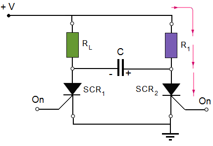
This reverse voltage causes the forward current through SCR1 to drop below its holding value thus causing this SCR to turn off and remove power from RL.
Therefore a momentary gate current through SCR1 will turn on the circuit and a momentary gate current through SCR2 will turn off the circuit.
b) Thyristor as a power control:
SCR's may also be used to vary the amount of power applied to a load instead of just simply switching the power on or off.
In fact, they are widely used in power control applications where the source of power is 50 Hz AC. One of the most basic AC power control circuits which utilize an SCR is shown in Figure below. This circuit is commonly referred to as a half-wave phase control circuit. It uses just one SCR and it is capable of controlling the AC power applied to load resistor RL.
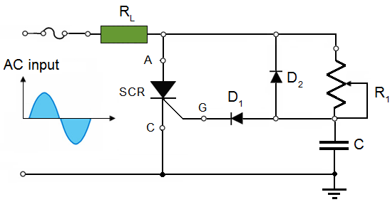
On each negative alternation of the input voltage, capacitor C charges through forward biased diode D2 and the SCR is biased in the reverse direction so that it cannot conduct. Also, on each negative alternation, diode D1 is reverse-biased and will not allow gate current to flow through the SCR.
During each positive alternation the SCR is forward-biased so that it can conduct forward current through RL if its gate current is high enough to turn it on.
However, the SCR's gate current is controlled by resistor R1 and capacitor C. This capacitor will discharge and then recharge through R1 during the positive alternations since D2 is reverse-biased during these portions of the AC cycle.
If the resistance of R1 is set to zero, capacitor C will charge almost immediately and the voltage across capacitor C (which is connected to the SCR's gate through D1) will quickly rise to a level which will cause the SCR to turn on.
In fact, when RM is equal to zero the SCR will turn on almost at the beginning of each positive alternation and apply power to RL for the entire alternation. Once the SCR turns on it will not turn off until the AC input voltage drops to zero.
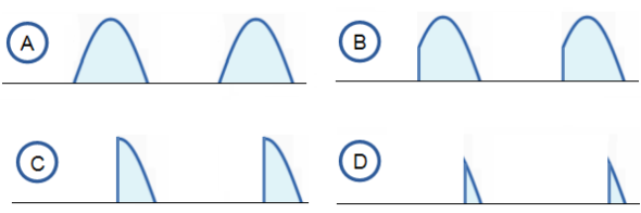
When RM is equal to zero the SCR simply acts like an ordinary junction diode and conducts during each positive alternation of the input AC voltage. This causes the voltage across RM to appear as shown in the figure A.
When the resistance RM is increased slightly, capacitor C cannot discharge and then recharge as quickly during each positive alternation. This means that it will take slightly longer for the voltage across capacitor C to rise to a level which will cause the SCR to turn on. SCR turns on shortly after each positive alternation has started and not at the beginning of each alternation as it did before. This causes the voltage across RM to appear as shown in figure B.
The resistance RM can be further increased to further extend the time required for the SCR to turn on during each positive alternation. Figure C shows the voltage across RM when RM is increased to the point where the SCR conducts for only half of each positive alternation.
Figure D shows the voltage across RM when RM is made even larger.
If the value of RM is increased further, the SCR will not conduct at all and no power will be applied to RM.
2. DIAC:
2.1. Diac symbol and composition:
The diac is a bidirectional trigger diode that conducts current only after its breakdown voltage has
been exceeded momentarily. It stops conducting when the current through it drops below a value characteristic for the device. The behaviour is typically the same for both directions of current flow.
The diagram to the right shows the resulting five-layer device, which is known as a diac. At first glance, it seems unreasonable or even impossible, considering that each connection to the semiconductor crystal overlaps a PN junction. However, the device does work, and indeed works well.
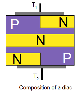
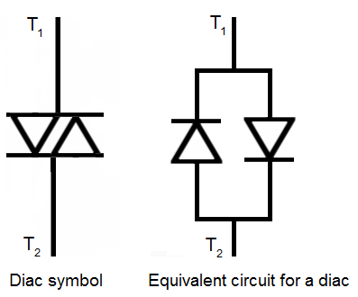
The terms anode and cathode no longer apply, so the connections are simply named terminal 1 (T1) and terminal 2 (T2). Each terminal can serve as either anode or cathode, according to the polarity of the applied voltage.
That same applied polarity also determines which of the end junctions is active, and which one is bypassed. Thus, if T1 is positive with respect to T2, T1's N-type region is ignored (electrons are pulled away from that junction) and its P-type region serves as the anode.
At the same time, the relative negative voltage at T2 pulls holes from the P-type region towards the terminal (removing them from the next junction), but tends to push electrons from its N-type region across that junction into the P-type region, thus making them available for conduction.
The diac, like the four-layer diode, remains non-conducting until its breakover voltage is reached, at which point it turns on fully and remains on until the applied voltage or circuit current are reduced below the holding values at which conduction can be maintained.
Since the diac is normally used in ac circuits, operating as part of the control circuit for devices powered from a household wall socket or similar source, this is not a problem.
2.2. Diac characteristics:
Although most diacs have symmetric switching voltages, asymmetric diacs are available. Typical diacs have a power dissipations ranging from 1/2 to 1 watt.
The main characteristics are:
Breakover voltage, generally from 20 to 40 volts,
Breakover current, generally from 50 to 200 milliamperes
Power dissipation, generally from ½ to 1 watt.
IDRM is the leakage current of the diac with VDRM applied from T2 to T1 and is several orders of magnitude smaller than the current rating of the device.
3. TRIAC:
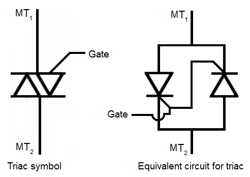
The bidirectional triode thyristor (triac) is a solid-state device that acts like two SCRs that have been connected in parallel with each other (inversely) so that one SCR will conduct the positive half-cycle and the other will conduct the negative half-cycle. This means that the triac can be used for control in AC circuits. Before the triac was designed as a single component, two SCRs were actually used for this purpose.
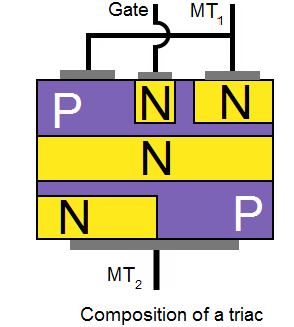
3.1. Triac symbol and composition:
Figure shows the symbol for the triac, and its PN structure. The terminals of the triac are identified as main terminal 1 (MT1), main terminal 2 (MT2), and gate. The multiple PN structure is actually a combination of two four-layer (PNPN) junctions.
The triac offers the circuit designer an economical and versatile means of accurately controlling ac power. It has several advantages over conventional mechanical switches.
Since the triac has a positive “on” and a zero current “off” characteristic, it does not suffer from the contact bounce or arcing inherent in mechanical switches.
The switching action of the triac is very fast compared to conventional relays, giving more accurate control. A triac can be triggered by AC, DC, rectified AC or pulses. Because of the low energy required for triggering a triac, the control circuit can use any of many low-cost solid-state devices such as transistors, bilateral switches, sensitive gate SCRs and triacs, optically coupled drivers and integrated circuits.
3.2. Triac characteristics:
To avoid confusion, it has become standard practice to specify all currents and voltages using MT1 as the reference point.
The triac is a five layer device with the region between T1 and T2 being P−N−P−N switch (SCR) in parallel with a N−P−N−P switch (complementary SCR).
Also, the structure gives some insight into the triac's ability to be triggered with either a positive or negative gate signal. The region between MT1 and G consists of two complementary diodes. A positive or negative gate signal will forward−bias one of these diodes causing the same transistor action found in the SCR.
This action breaks down the blocking junction regardless of the polarity of MT1. Current flow between MT2 and MT1 then causes the device to provide gate current internally. It will remain on until this current flow is interrupted.
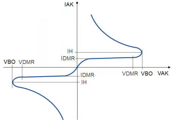
The voltage current characteristic of the triac is shown in Figure below where, as previously stated, MT1 is used as the reference point. The first quadrant, Q1, is the region where MT2 is positive with respect to MT1 and quadrant III is the opposite case.
Several of the terms used in characterizing the triac are shown on the figure. VDRM is the breakover voltage of the device and is the highest voltage the triac may be allowed to block in either direction. If this voltage is exceeded, even transiently, the triac may go into conduction without a gate signal.

Although the triac is not damaged by this action if the current is limited, this situation should be avoided because control of the triac is lost. A triac for a particular application should have VDRM at least as high as the peak of the ac waveform to be applied so reliable control can be maintained. The holding current (IH) is the minimum value of current necessary to maintain conduction.
When the current goes below IH, the triac ceases to conduct and reverse to the blocking state. IDRM is the leakage current of the triac with VDRM applied from MT2 to MT1 and is several orders of magnitude smaller than the current rating of the device.
The figure shows the characteristic of the triac without a gate signal applied but it should be noted that the triac can be triggered into the on state at any value of voltage up to VDRM by the application of a gate signal. This important characteristic makes the triac very useful.
Since the triac will conduct in either direction and can be triggered with either a positive or negative gate signal there are four possible triggering modes:
Quadrant 1; MT2 (+), G(+), positive voltage and positive gate current.
Quadrant 2; MT2(+), G(−), positive voltage and negative gate current.
Quadrant 3; MT2 (−), G(−), negative voltage and negative gate current.
Quadrant 4; MT2 (−), G(+), negative voltage and positive gate current.
Present triacs are most sensitive in quadrants 1 and 3, slightly less so in quadrant 2, and much less sensitive in quadrant 4. Therefore it is not recommended to use quadrant 4 unless special circumstances dictate it.
An important fact to remember is that since a triac can conduct current in both directions, it has only a brief interval during which the sine wave current is passing through zero to recover and revert to its blocking state.
For this reason, reliable operation of present triacs is limited to 50/60 Hz line frequency and lower frequencies.
For inductive loads, the phase shift between the current and voltage means that at the time the current falls below IH and the triac ceases to conduct, there exists a certain voltage which must appear across the triac.
If this voltage appears too rapidly, the triac will resume conduction and control is lost. In order to achieve control with certain inductive loads, the rate of rise in voltage must be limited by a series RC network across the triac.
The capacitor will then limit the rate of rise in voltage across the triac.
The resistor is necessary to limit the surge of current from the capacitor when the triac fires, and to damp the ringing of the capacitance with the load inductance.
3.3. Phase control with thyristor (diac and triac):
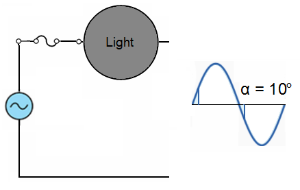
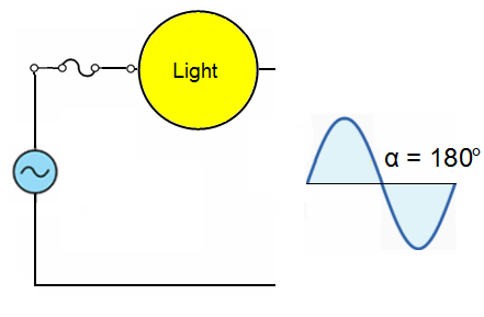
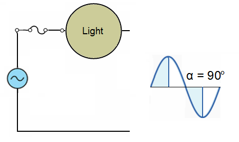
The most common method of electronic AC power control is called phase control. Figure illustrates this concept. During the first portion of each half-cycle of the AC sine wave, an electronic switch is opened to prevent the current flow.
At some specific phase angle α, this switch is closed to allow the full line voltage to be applied to the load for the remainder of that half-cycle. Varying α will control the portion of the total sine wave that is applied to the load (shaded area), and thereby regulate the power flow to the load.
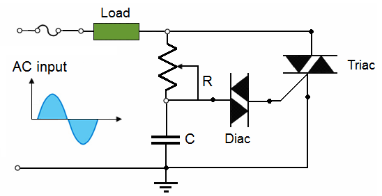
The electronic switch in this case is a triac which can be turned on by a small current pulse to its gate. The triac turns off automatically when the current through it passes through zero. In the circuit shown, capacitor C is charged during each half-cycle by the current flowing through resistor R and the load.
The fact that the load is in series with R during this portion of the cycle is of little consequence since the resistance of R is many times greater than that of the load.
When the voltage across C reaches the breakdown voltage of the diac bilateral trigger (D), the energy stored in capacitor C is released.
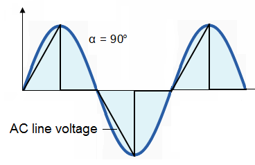
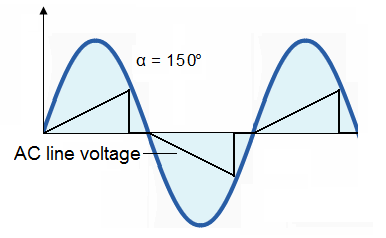
This energy produces a current pulse in the diac, which flows through the gate of the triac and turns it on.
Since both the diac and the triac are bidirectional devices, the values of R and C will determine the phase angle at which the triac will be triggered in both the positive and negative half-cycles of the AC sine wave.
The waveform of the voltage across the capacitor for two typical control conditions ( α= 90° and 150°) is shown in Figure. If a silicon controlled rectifier is used in this circuit in place of the triac, only one half-cycle of the waveform will be controlled. The other half-cycle will be blocked, resulting in a pulsing dc output whose average value can be varied by adjusting R.
3.4. Example of application: - the dimmer:
a) The old way:
Early dimmer switches had a pretty straightforward solution to adjusting light levels a variable resistor.
An ordinary resistor is a piece of material that doesn't conduct electrical current well it offers a lot of resistance to moving electrical charge. A variable resistor consists of a piece of resistive material, a stationary contact arm and a moving contact arm.
In this design, you vary the total resistance of the resistor by adjusting the distance that the charge has to travel through resistive material. If the contact arm is to the left, charge flowing through the circuit only has to travel through a little bit of resistive material. If the contact arm is all the way to the right, the charge has to move through more resistive material.
As the charge works to move through the resistor, energy is lost in the form of heat.
When you put a resistor in a series circuit, the resistor's energy consumption causes a voltage drop in the circuit, decreasing the energy available to other loads (the light bulb, for example). Decreased voltage across the light bulb reduces its light output.
The problem with this solution is that you end up using a lot of energy to heat the resistor, which doesn't help you light up the room but still costs you. In addition to be being inefficient, these switches tend to be cumbersome and potentially dangerous, since the variable resistor releases a substantial amount of heat.
b) The modern way:
At first triac is not conducting; C is charged through potentiometer until the trigger level of diac is reached. When the diac trigger level is reached (about 30 V), diac fires and triac is switched on.
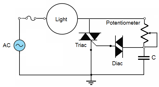
The triac will remain in conductive mode until the mains current is lower than the triac hold current at the end of the half mains period.
This works for both the negative and positive mains period because both the triac and the diac are bi-directional.
The fuse is absolutely mandatory as the discharge arc in a failing incandescent lamp is virtually a short circuit.
If you do not have a diac you can replace it with a small neon lamp (without series resistor) but then you will have to use a smaller value for P1 because the "trigger" voltage of a small neon lamp is higher: typically 70 V.
c) Dimmer switch schematic:
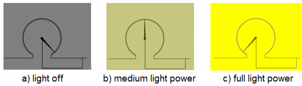
At full brilliance:
When the potentiometer is set to minimum, the capacitor charges up instantly.
So the TRIAC is triggered when the live is about 30V, and stays on, lighting the lamp until the mains is gone to zero volts at the end of the 1/2 cycle.
At half power:
When the potentiometer is about half way around, the capacitor reaches 30V around 1/2 way along the 1/2 cycle when triggering occurs. This still produces the full peak voltage only half the energy is delivered to the lamp.
At max dimming:
When the pot is at maximum the 0.1uF cap only just charges up 30V near the end of the 1/2 cycle. The triac is then triggered and provides the very low voltage mains at the end of the 1/2 cycle to the lamp, until Zero volts releases the triac ready for re-triggering.